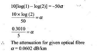
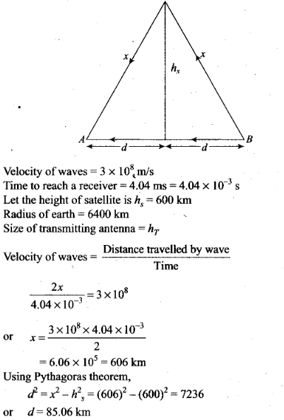
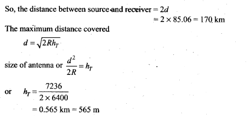
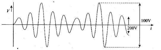
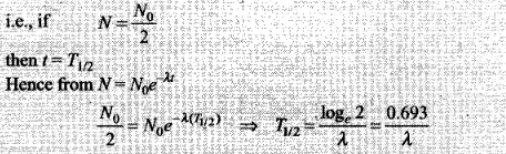
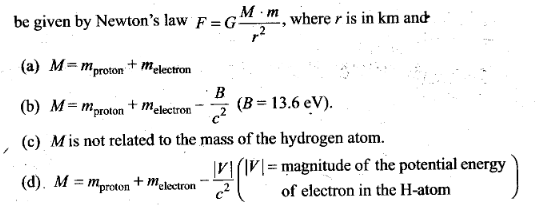
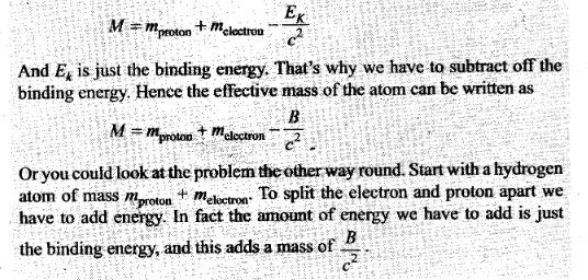
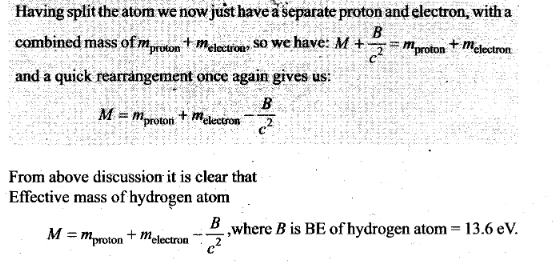
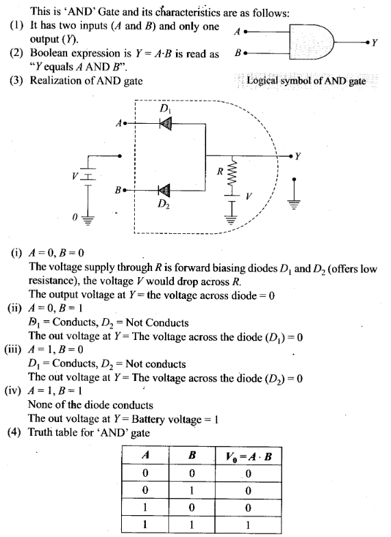
NCERT Exemplar Problems Class 12 Physics Chapter 14 Semiconductor Electronics: Materials, Devices and Simple Circuits
Multiple Choice Questions (MCQs)
Single Correct Answer Type
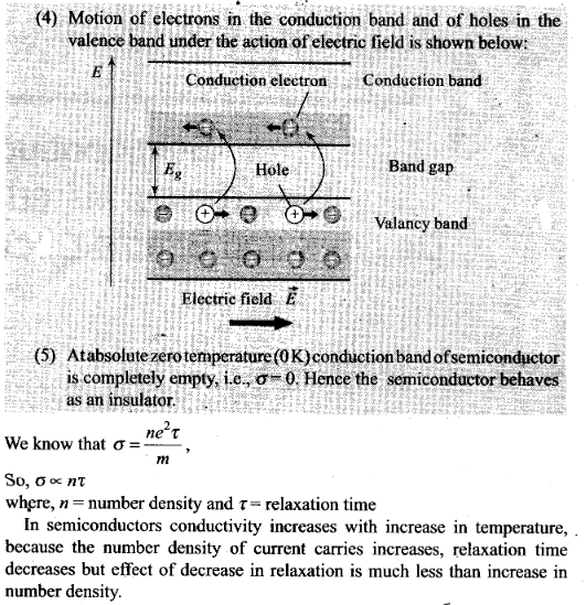
Question 1. The conductivity of a semiconductor increases with increase in temperature, because
(a) number density of free current carries increases
(b) relaxation time increases
(c) both number density of carries and relaxation time increase
(d) number density of carries increases, relaxation time decreases but effect of decrease in relaxation time is much less than increase in number density .
Solution: (d)
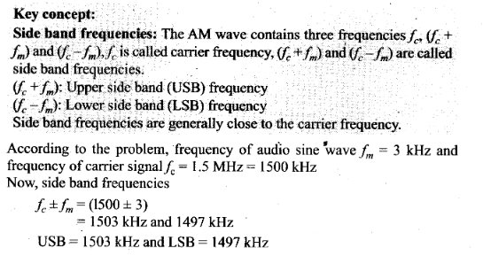
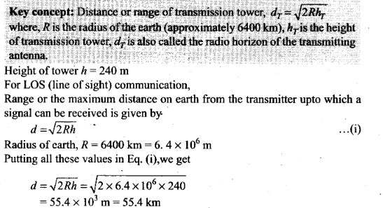
Question 2.
Solution: (b)
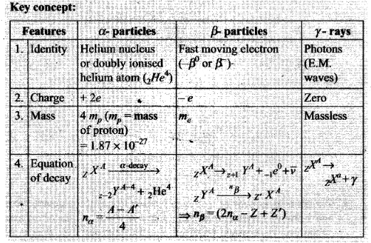
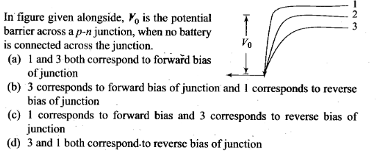
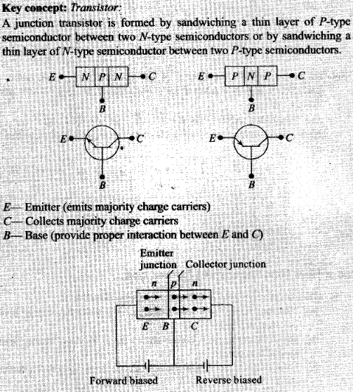
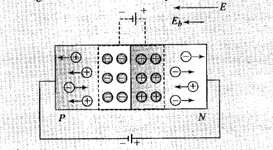
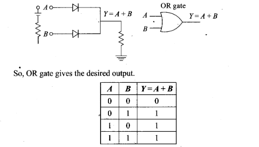
Key concept: P-N Junction Diode:
– When a P-type semiconductor is suitably joined to an N-type semiconductor, then resulting arrangement is called P-N junction or P-N junction diode.
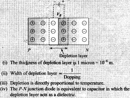
(1) Depletion region: On account of difference in concentration of charge carrier in the two sections of P-N junction, the electrons from N-region diffuse through the junction into P-region and the hole from P region diffuse into N-region.
Due to diffusion, neutrality of both N and P-type semiconductor is disturbed, a layer of negative charged ions appear near the junction in the P-crystal and a layer of positive ions, appears near the junction in N-crystal. This layer is called depletion layer.
(2) Potential barrier: The potential difference created across the P-N junction due to the diffusion of electron and holes is called potential barrier.
Height of potential barrier is decreases when p-n junction is forward biased, it opposes the potential barrier junction, when p-n junction is reverse biased, it supports the potential barrier junction, resulting increase in potential barrier across the junction.
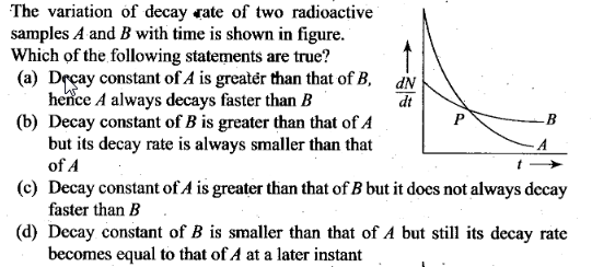
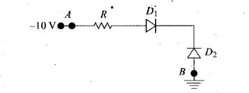
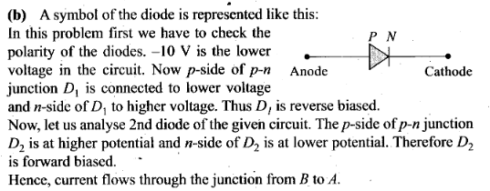
Question 3. In figure given on next page, assuming the diodes to be ideal
(a) D1 is forward biased and D2 is reverse biased and hence current flows from A to B
(b) D2 is forward biased and D1 is reverse biased and hence no current flows from B to A and vice-versa
(c) D1 and D2 are both forward biased and hence current flows from A to B
(d) D1 and D2 are both reverse biased and hence no current flows from A to B and vice-versa
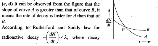
Solution:
Question 4. A 220 V AC supply is connected between points A and B (figure). What will be the potential difference V across the capacitor?
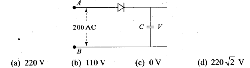
Solution: (d)
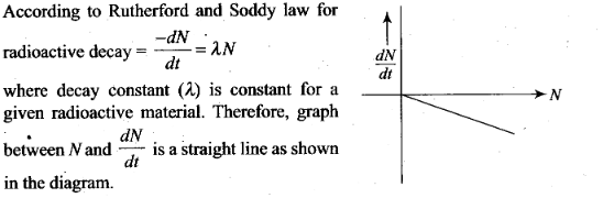
Key concept: Half wave rectifier: When the P-N junction diode rectifies half of the ac wave, it is called half wave rectifier.
Question 5. Hole is
(a) an anti-particle of electron
(b) a vacancy created when an electron leaves a covalent bond
(c) absence of free electrons
(d) an artificially created particle
Solution: (b) Concept of holes in the semiconductor:
- .When an electron is removed from a covalent bond, it leaves a vacancy behind. An electron from a neighbouring atom can move into this vacancy, leaving the neighbour with a vacancy. In this way the vacancy formed is called a hole (or cotter), and can travel through the material and serve as an additional current carriers.
- A hole is considered as a seat of positive charge, having magnitude of charge equal to that of an electron.
- Holes acts as a virtual charge, although there is no physical charge on it.
- Effective mass of hole is more than an electron.
- Mobility of hole is less than an electron.
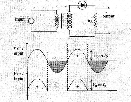
Question 6. The output of the given circuit in figure is given below.
(a) would be zero at all times
(b) would be like a half wave rectifier with positive cycles in output
(c) would be like a half wave rectifier with negative cycles in output
(d) would be like that of a full wave rectifier
Solution: (c)
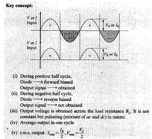
When the diode is forward biased during positive half cycle of input AC voltage, the resistance of p-n junction is low. The current in the circuit is maximum. In this situation, a maximum potential difference will appear across resistance connected in a series of circuit. This result into zero output voltage across p-n junction.
And when the diode is reverse biased during negative half cycle of AC voltage, the p-n junction is reverse biased. The resistance of p-n junction becomes high which will be more than resistance in series. That is why, there will be voltage across p-n junction with negative cycle in output, hence option (c) is correct.
Question 7. In the circuit shown in figure given below, if the diode forward voltage between A and B is
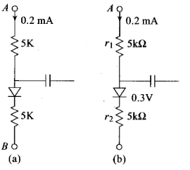
(a) 1.3 V (b) 2.3 V (c) 0 (d) 0.5 V
Solution:
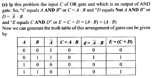
Question 8. Truth table for the given circuit is
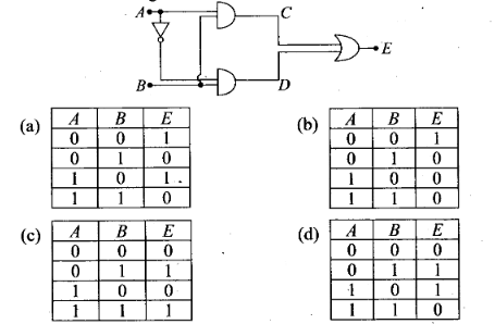
Solution:
One or More Than One Correct Answer Type
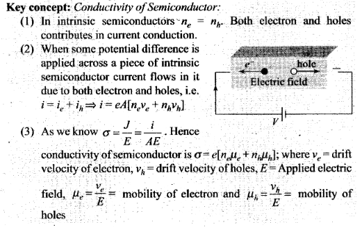
Question 9. When an electric field is applied across a semiconductor
(a) electrons move from lower energy level to higher energy level in the conduction band
(b) electrons move from higher energy level to lower energy level in the conduction band
(c) holes in the valence band move from higher energy level to lower energy level
(d) holes in the valence band move from lower energy level to higher energy level
Solution: (a, c)
In valence band electrons are not capable of gaining energy from external electric field. While in conduction band the electrons can gain energy from external electric field.
When electric field is applied across a semiconductor, the electrons in the conduction band (which is partially filled with electrons) get accelerated and acquire energy. They move from lower energy level to higher energy level. While the holes in valence band move from higher energy level to lower energy level, where they will be having more energy.
Question 10. Consider an n-p-n transistor with its base-emitter junction forward biased and collector base junction reverse biased. Which of the following statements are true?
(a) Electrons crossover from emitter to collector
(b) Holes move from base to collector
(c) Electrons move from emitter to base
(d) Electrons from emitter move out of base without going to the collector.
Solution: (a, c)
In normal operation base-emitter is forward biased, i.e., the positive pole of emitter base battery is connected to base and its negative pole is connected to the emitter. And collector base junction is reverse biased, i.e., the positive pole of the collector base battery is connected to collector and negative pole to base. Thus, electron moves from emitter to base and crossover from emitter to collector.
Question 11.
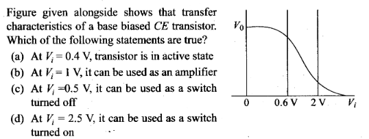
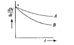
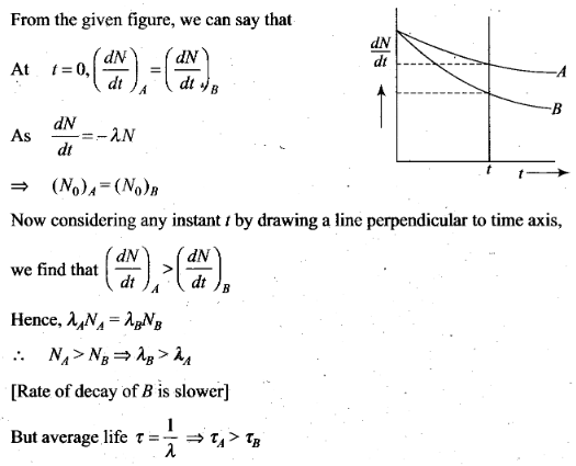
Solution: (b, c, d) According to above graph transfer characteristics of a base biased common emitter transistor, we note that .
(a) when Vi= 0.4 V, output voltage remain same,there is no collection current. So, transistor circuit is not in active state.
(b) when Vi = 1 V (This is in between 0.6 V to 2 V), the transistor circuit is in active state and when input is increasing output is decreasing because when CE is used as an amplifier input and output voltages are 180° out of phase. Then it is used as an amplifier.
(c) when Vi = 0.5 V, there is no collector current. The transistor is in cut off state. The transistor circuit can be used as a switch to be turned off.
(d) when Vi = 2.5 V, the collector current becomes maximum and transistor is in a saturation state and can used as switch turned on state.
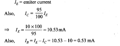
Question 12. In a n-p-n transistor circuit, the collector current is 10 mA. If 95 per cent of the electrons emitted reach the collector, which of the following statements are true?
(a) The emitter current will be 8 mA
(b) The emitter current will be 10.53 mA
(c) The base current will be 0.53 mA
(d) The base current will be 2 mA
Solution: (b, c) According to the problem, the collector current is 95% of electrons reaching the collector after emission. And collector current, IC = 10 mA
Question 13. In the depletion region of a diode
(a) there are no mobile charges
(b) equal number of holes and elections exist, making the region neutral
(c) recombination of holes and electrons has taken place
(d) immobile charged ions exist
Solution: (a, b, d) On account of difference in concentration of charge carrier in the two sections of P-N junction, the electrons from N-rcgion diffuse through the junction into P-region and the hole from P-region diffuse into N-region.
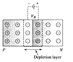
Due to diffusion, neutrality of both N-and P-type semiconductor is disturbed, a layer of negative charged ions appear near the junction in the P-crystal and a layer of positive ions appears near the junction in N-crystal. This layer is called depletion layer.
The thickness of depletion layer is 1 micron = 10-6 m.
Width of depletion layer ∞ 1/Dopping
Depletion is directly proportional to temperature.
Important point: The P-N junction diode is equivalent to capacitor in which the depletion layer acts as a dielectric.
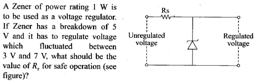
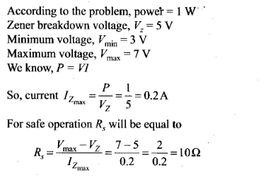
Question 14. What happens during regulation action of a Zener diode?
(a) The current and voltage across the Zener remains fixed
(b) The current through the series Resistance (Rs) changes
(c) The Zener resistance is constant
(d) The resistance offered by the Zener changes
Solution: (b, d) Symbolically zener diode represents like this:
In the forward bias, the zener diode acts as an ordinary diode. It can be used as a voltage regulator.
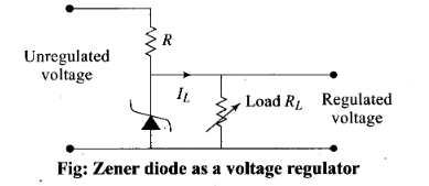
A zener diode when reverse biases offers constant voltage drop across in terminals as unregulated voltage is applied across circuit to regulate. Then during regulation action of a Zener diode, the current through the series resistance Rs changes and resistance offered by the Zener changes. The current through the Zener changes but the voltage across the Zener remains constant.
Question 15. To reduce the ripples in rectifier circuit with capacitor filter
(a) RL should be increased
(b) input frequency should be decreased .
(c) input frequency should be increased
(d) capacitors with high capacitance should be used
Solution: (a, c, d)
Ripple factor may be defined as the ratio of r.m.s. value of the ripple voltage to the absolute value of the DC component of the output voltage, usually expressed as a percentage. However ripple voltage is also commonly expressed as the peak-to-peak value. Ripple factor (r) of a full wave rectifier using capacitor filter is given by
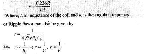
Ripple factor is inversely proportional to RL, C and v.
Thus to reduce r, RL should be increased, input frequency v should be increased and capacitance C should be increased.
Question 16. The breakdown in a reverse biased p-n junction is more likely to occur due to
(a) large velocity of the minority charge carriers if the doping concentration is small
(b) large velocity of the minority charge carriers if the doping concentration is large
(c) strongelectricfieldinadepletionregionifthedopingconcentrationissmall
(d) strong electric field in the depletion region if the doping concentration is large
Solution: (a, d)
Reverse biasing: Positive terminal of the battery is connected to the N-crystal and negative terminal of the battery is connected to P-crystal.
(i) In reverse biasing width of depletion layer increases
(ii) In reverse biasing resistance offered RReverse = 105 Ω
(iii) Reverse bias supports the potential barrier and no current flows across the junction due to the diffusion of the majority carriers.
(A very small reverse current may exist in the circuit due to the drifting of minority carriers across the junction)
(iv) Break down voltage: Reverse voltage at which break down of semiconductor occurs. For Ge it is 25 V and for Si it is 35 V.
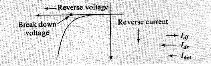
So, we conclude that in reverse biasing, ionization takes place because the minority charge carriers will be accelerated due to reverse biasing and striking with atoms which in turn cause secondary electrons and thus more number of charge carriers.
When doping concentration is large, there will be a large number of ions in the depletion region, which will give rise to a strong electric field.
Very Short Answer Type Questions
Question 17. Why are elemental dopants for Silicon or Germanium usually chosen from group XIII or group XV?
Solution: When pure semiconductor material is mixed with small amounts of certain specific impurities with valency different from that of the parent material, the number of mobile electrons/holes drastically changes. The process of addition of impurity is called doping. The size of the dopant atom should be compatible such that their presence in the pure semiconductor does not distort the semiconductor but easily contribute the charge carriers on forming covalent bonds with Silicon or Germanium atoms, which are provided by group XIII or group XV elements.
Question 18. Sn, C and Si, Ge are all group XIV elements. Yet, Sn is a conductor, C is an insulator while Si and Ge are semiconductors. Why?
Solution: The conduction level of any element depends on the energy gap between its conduction band and valence band.
In conductors, there is no energy gap between conduction band and valence band. For insulator, the energy gap is large and for semiconductor the energy gap is moderate.
The energy gap for Sn is 0 eV, for C is 5.4 eV, for Si is 1.1 eV and for Ge is 0.7 eV related to their atomic size. Therefore Sn is a conductor, C is an insulator, and Ge and Si are semiconductors
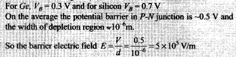
Question 19. Can the potential barrier across a p-n junction be measured by simply connecting a voltmeter across the junction?
Solution: We cannot measure the potential barrier across a p-n junction by a voltmeter because the resistance of voltmeter is very high as compared to the junction resistance. Potential of potential barrier for Ge is VB = 0.3 V and for silicon is VB = 0.7 V.
On the average the potential barrier in P-N junction is ~0.5 V.
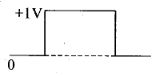
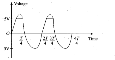
Question 20. Draw the output waveform across the resistor in the given figure.
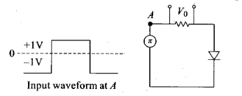
Solution: The diode act as a half wave rectifier, it offers low resistance when forward biased and high resistance when reverse biased. So the output is obtained only when positive input is given,so the output waveform is
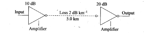
Question 21. The amplifiers X, Y and Z are connected in series. If the voltage gains of X, Y and Z are 10,20 and 30, respectively and the input signal is 1 mV peak value, then what is the output signal voltage (peak value).
(i) if DC supply voltage is 10 V?
(ii) if DC supply voltage is 5 V?
Solution: Total voltage amplification is defined as the ratio of output signal voltage and input signal voltage.
Question 22. In a CE transistor amplifier, there is a current and voltage gain associated with the circuit. In other words there is a power gain. Considering power a measure of energy, does the circuit violate conservation of energy?
Solution:
The power gain is very high in CE transistor amplifier. In this circuit, the extra power required for amplified output is obtained from DC source. Thus, the circuit used does not violate the law of conservation.
Short Answer Type Questions
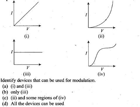
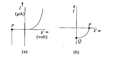
Question 23. (i) Name the type of a diode whose characteristics are shown in figure (a) and (b).
(ii) What does the point P in fig. (a) represent?
(iii) What does the points P and Q in fig. (b) represent?
Solution:
(i) Fig. (a) represents the characteristics of Zener diode and curve (b) is of solar cell.
(ii) In fig. (a), point P represents Zener breakdown voltage.
(iii) In fig. (b), the point Q represents zero voltage and negative current. Which means the light falling on solar cell with atleast minimum threshold frequency gives the current in opposite direction to that due to a battery connected to solar cell. But for the point Q the battery is short circuited. Hence it represents the short circuit current.
And the point Pin fig. (b) represents some open circuit, voltage on solar cell with zero current through solar cell.
It means, there is a battery connected to a solar cell which gives rise to the equal and opposite current to that in solar cell by virtue of light falling on it.
Question 24. Three photo diodes D1, D2 and D3 are made of semiconductors having band gaps of 2.5 eV, 2 eV and 3 eV, respectively. Which ones will be able to detect light of wavelength 6000 Å ?
Solution:Key concept: In Photo diodes electron and hole pairs are created by junction photoelectric effect. That is the covalent bonds are broken by the EM radiations absorbed by the electron in the V.B. These are used for detecting light signals.
The incident radiation which is detected by the photodiode D2 because energy of incident radiation is greater than the band-gap.
Question 25. If the resistance R1 is increased (see figure), how will the readings of the ammeter and voltmeter change?
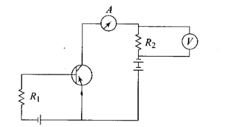
Solution: Let us redrawn the circuit diagram to find the change in reading of ammeter and voltmeter.
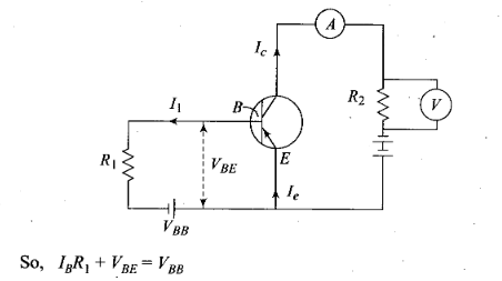
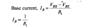
So, R1 is increased, IB is decreased.
Now, the current in ammeter is collector current IC.
IC =βIB as IB is decreased, IC is also decreased and the reading of voltmeter and ammeter also decreased.
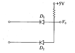
Question 26. Two car garages have a common gate which needs to open automatically when a car enters either of the garages or cars enter both. Draw a circuit that resembles this situation using diodes for this situation.
Solution: As car enters in either of the garages or both, the common gate opened automatically.
This means that if any one input is high, output will high otherwise low.
The device is shown like this:
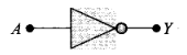
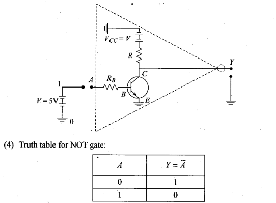
Question 27. How would you set up a circuit to obtain NOT gate using a transistor?
Solution:
(1)It has only one input and only one output.
(2)Boolean expression is Y = Ᾱ and is read as “y equals not A” .
Logical symbol of NOT gate.
(3)Realization of NOT gate: The transistor is so biased that the collector voltage VCC = V (Voltage corresponding to 1 state)
The resistors R and RB are so chosen that if the input is low, i.e. 0, the transistor is in the cut off and hence the voltage appearing at the output will be the same as applied V = 5 V. Hence Y= V(or state I)
If the input is high, the transistor current is in saturation and the net voltage at the output Y is 0 (in state 0).
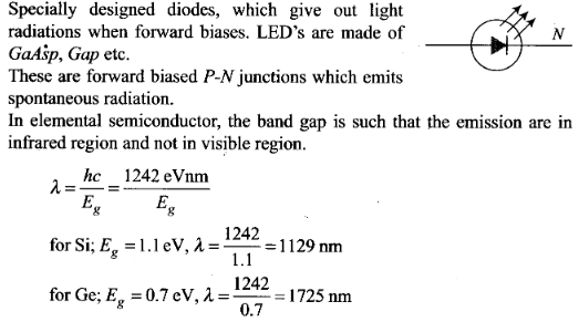
Question 28. Explain why elemental semiconductor cannot be used to make visible LEDs.
Solution:
Question 29. Write the truth table for the circuit shown in figure given below. Name the gate that the circuit resembles.
Solution:
Question 30.
Solution:
Long Answer Type Questions
Question 31. If each diode in figure has a forward bias resistance of 25 Ω and infinite resistance in reverse bias, what will be the values of the currents I1, I2, I3 and I4?
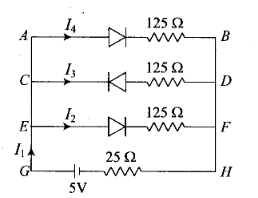
Solution:
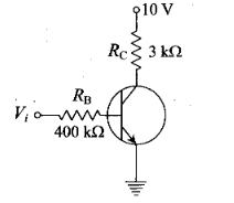
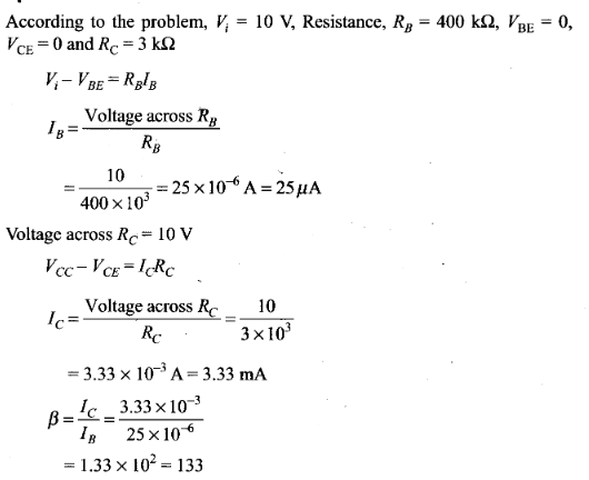
Question 32. In the circuit shown in figure, when the input voltage of the base resistance is 10 V, VBE is zero and VCE is also zero. Find the values of IB, IC and β .
Solution:
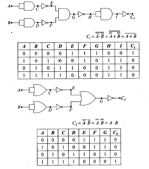
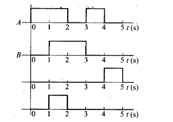
Question 33. Draw the output signals C1 and C2 in the given combination of gates.
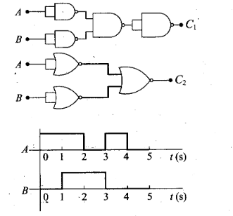
Solution:
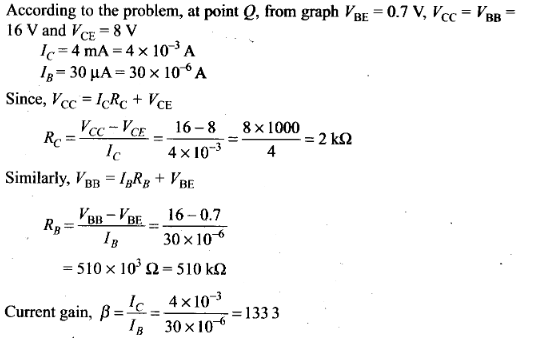
Question 34. Consider the circuit arrangement shown in figure for studying input and output characteristics of n-p-n transistor in.CE configuration.
Select the values of RB and RC for a transistor whose VBE = 0.7 V so that the transistor is operating at point Q as shown in the characteristics (see figure).
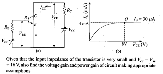
Solution:
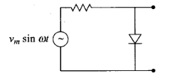
Question 35. Assuming the ideal diode, draw the output waveform for the circuit given in figure, explain the waveform.
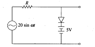
Solution:
Key concept: An ideal diode is a diode in which it has a very large resistance in reverse biased and very, low resistance in forward biased. So, it acts like a perfect conductor when voltage is applied forward biased and like a perfect insulator when voltage is applied reverse biased.
In reverse biased when the input voltage is equal to or less than 5 V diode,then it will offer high resistance in comparison to resistance (R) in series. Now, diode appears in open circuit. The input waveform is then passed to the output terminals. The result with sin wave input is to dip off all positive going portion above 5 V.
If input voltage is greater than +5 V, diode is in conducting state, then it will be conducting as if forward biased offering low resistance in comparison to R. But there will be no voltage in output beyond 5 V as the voltage beyond +5 V will appear across R.
When input voltage is negative, there will be opposition to 5 V battery in p-n junction input voltage becomes more than -5 V, the diode will be reverse biased. It will offer high resistance in comparison to resistance R in series. Now junction diode appears in open circuit. The input wave form is then passed on to the output terminals.
The output waveform will be like this (as shown below).
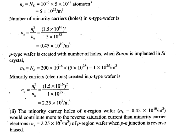
Question 36. Suppose a n-type wafer is‘created by doping Si crystal having 5 x 1028 atoms/m3 with 1 ppm concentration of As. On the surface 200 ppm boron is added to create ‘p’ region in this wafer. Considering ni = 1.5 x 10¹⁶ m-3,
(i) Calculate the densities of the charge carriers in the n and p regions,
(ii) Comment which charge carriers would contribute largely for the reverse saturation current when diode is reverse biased.
Solution: n-type wafer is created when As is implanted in Si crystal. The number of majority carriers electrons due to doping of As is
Question 37. An XOR gate has the following truth table.
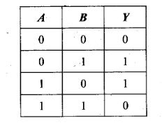
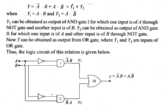
It is represented by following logic relation Y = Ᾱ . B + A . B’ . Build this gate using AND, OR and NOT gates.
Solution: XOR gate can be realized by the combination of two NOT gates, two AND gates and one OR gate. According to the problem, the logic relation for the . given truth table is
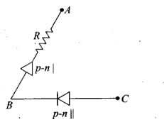
Question 38. Consider a box with three terminals on top of it as shown in figure.
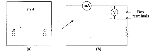
Three components namely, two germanium diodes and one resistor are connected across these three terminals in some arrangement.
A student performs an experiment in which any two of these three terminals are connected in the circuit as shown in figure.
The student obtains graphs of current-voltage characteristics for unknown combination of components between the two terminals connected in the circuit. The graphs are
(i) when A is positive and B is negative .
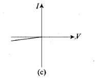
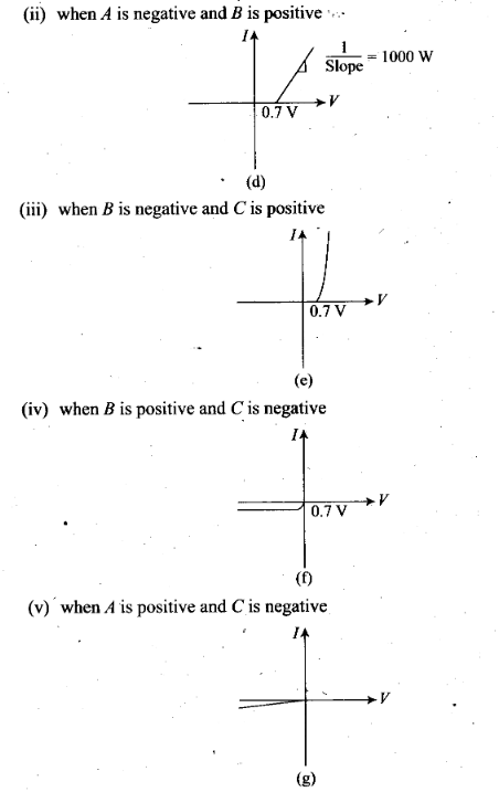
Solution: The V-I characteristics of these graph is discussed in points:
(a)In V-I graph of condition (i), a reverse characteristics is shown in fig. (c). Here A is connected to n-side of p-n junction I and B is connected top-side of p-n junction I with a resistance in series.
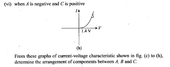
(b)In V-I graph of condition (ii), a forward characteristics is shown in fig. (d), where 0.7 V is the knee voltage of p-n junction I. 1/slope = (1/1000) Ω.
It means A is connected to n-side of p-n junction I and B is connected to p-side of p-n junction I and resistance R is in series of p-n junction I between A and B.
(c)In V-I graph of condition (iii), a forward characteristics is shown in figure (e) , where 0.7 V is the knee voltage. In this case p-side of p-n junction II is connected to C and n-side of p-n junction II to B.
(d)In V-I graphs of conditions (iv), (v), (vi) also concludes the above connection of p-n junctions I and II along with a resistance R.
Thus, the arrangement of p-n I, p-n II and resistance R between A, B and C will be as shown in the figure.
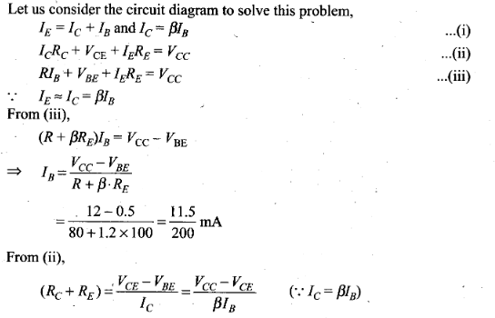
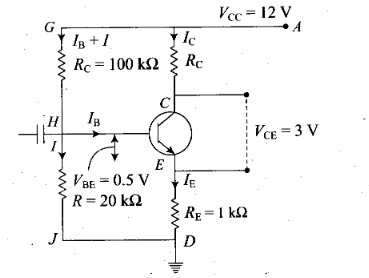
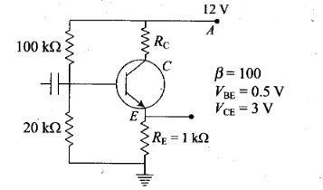
Question 39. For the transistor circuit shown in figure, evaluate VE, RB, RE, given IC= 1 mA, VCE= 3, VBE = 0.5 V and VCC= 12 V, β= 100.
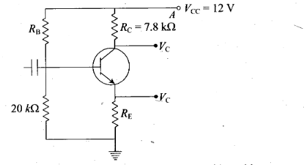
Solution: Let us redraw the circuit diagram given here to solve this problem.
Question 40. In the circuit shown in figure, find the value of Rc .
.
Solution: